One of the Evolution of the Silicon Wafer Landscape
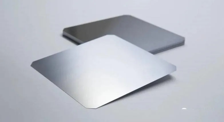
Monocrystalline silicon wafers have gradually replaced polycrystalline silicon wafers, and have now become the most mainstream type of silicon wafers. Accompanied by the continuous penetration of diamond wire cutting technology and the implementation of the domestic frontrunner program, according to statistics to 2023, China’s monocrystalline silicon wafer market share has reached 99.2%, monocrystalline silicon wafer has completed the replacement of polysilicon wafer.
The Evolution of the Silicon Wafer Landscape II
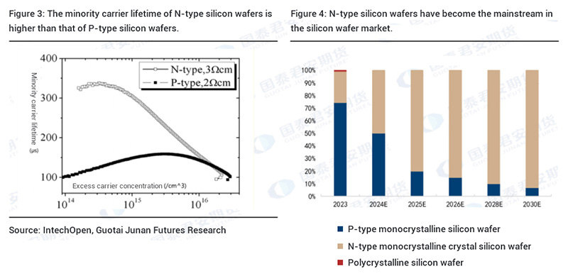
Monocrystalline silicon wafers N-type wafers gradually replace P-type wafers and develop into the mainstream of the industry. In monocrystalline silicon wafers, along with the photovoltaic industry to reduce costs and increase efficiency, N-type batteries to replace P-type batteries has become a major trend in the industry, and drive the N-type wafer penetration rate. According to statistics, since 2023, the proportion of N-type silicon wafers has continued to rise, and by April 2024, its single-month production accounted for about 75%, and has become the mainstream product type of PV silicon wafers.
Silicon wafer technology route development trend
In the context of cost reduction and efficiency, silicon wafer change to “large size” and “thin wafer” is the main.
On the size end, the larger the wafer size, the higher the monolithic power, which can increase equipment capacity and enhance the power of cells and modules, thus diluting the non-silicon cost per watt. Until 2019, almost all wafers are below 166mm in size, but along with the development of large-size wafers, their market share is compressed to less than 2%.The mainstream wafer sizes in the market in 2023 will be 182-square wafers, micro-rectangular wafers, and 210-square wafers, with 47.7%, 20.3%, and 20% of the market share, respectively.

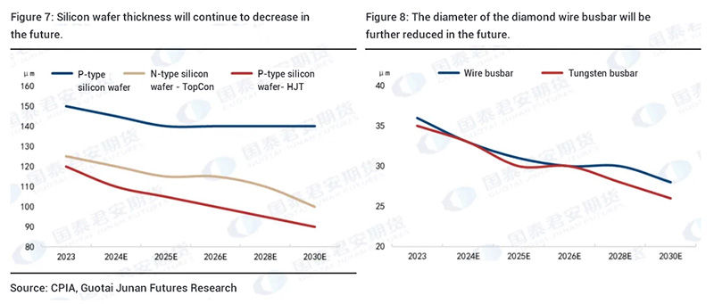
At the thickness end, the thinning of wafer thickness is conducive to reducing silicon consumption and wafer cost, thus achieving the purpose of cost reduction and efficiency. In recent years, under the wide application of diamond wire cutting technology, the thickness of photovoltaic silicon wafers has been reduced year by year. According to statistics as of 2023, the thickness of P-type monocrystalline silicon wafers has been reduced from 170 microns to 150 microns, while the thickness of N-type monocrystalline silicon wafers (used in TOPCon batteries) has been reduced from 165 microns to 125 microns, and the thickness of N-type monocrystalline silicon wafers (used in HJT batteries) has been reduced from 150 microns to 120 microns.

Monocrystalline silicon wafer production process has: melting, crystal pulling, slicing, grinding, cleaning and other processes
Slicing process: diamond wire cutting is the mainstream of the market
Diamond wire cutting is a plating method in the steel wire substrate deposited a layer of nickel metal, in the nickel metal layer wrapped with diamond particles, so that the diamond particles cemented in the steel wire substrate, and in the slicing process to complete the rapid pulling diamond wire wafer cutting. Diamond wire cutting process significantly reduces the cost of wire consumption, improve cutting speed and enhance the efficiency of slicing, etc., at the same time abandoned the expensive and environmentally friendly silicon carbide material, the cost advantage is more significant; in addition, due to the uniform thickness of the finished product of the diamond wire cutting, the product yield is also greatly improved.

JUNHE ® 2523 Diamond wire cutting fluid
1.Introduction
JUNHE® 2523 diamond abrasive wire cutting fluid maintains a low level of wire breakage, stable yield, and is adaptable to a variety of processes.
2.Features
- Good cleaning ability:Containing unique chemical cleaning additives, it makes the cut silicon wafer clean and easy to clean after cutting.
- Excellent lubrication ability:Excellent lubrication can effectively prevent brittle chipping or scratches from occurring on the wafer during the cutting process, reduce the surface roughness and surface warpage of the wafer, and minimize the total thickness deviation of the processed wafer.
- Environmental friendly:Selection of environmentally friendly materials, less foam, low cost of waste water treatment, easy to use.
- Good dispersion performance:Unique suspension to avoid silicon powder deposition to block the machine pipeline.
- Strong adaptability:Good compatibility, suitable for offline or large cycle.
3.Technical Parameters
| Item | Appearance | Density (20℃kg/L) | pH 5% aqueous solution | Rotational viscosity (25℃, mPa-s) | Surface tension (0.3% aqueous solution, mN/m) | Conductivity (1% aqueous solution, 25°C, us/cm) | COD (mg/L) |
| Reference | Colourless transparent liquid | 1.00±0. 10 | 5.0~7.0 | <200mPa.s | 20~35 | >1us/cm | ≤15,0000 |
| Testing reference standard | Visual assessment | ASTM D4052 | GB/T 23769 | GB/T5561 | GB/T22237 | GB/T6616-2009 | HJ 828 |
If the customer’s demand is within the parameter range of our products, we can specify the corresponding products.
Cleaning process
Silicon wafer in the cutting process, the surface will be covered with a layer of highly active suspension bond, very easy to form an oxide layer, while easy to adsorb all kinds of external impurities, such as organic pollutants, particles, inorganic impurities, metal ions, etc., these pollutants adsorbed on the surface of the wafer, cleaning is the sliced wafer cleaning, removal of impurities and pollutants on the surface to achieve the purpose of clean.
JUNHE ® 1015 Solar Silicon Wafer Cleaner
1.Introduction
JUNHE®1015 solar silicon wafer cleaner, silicon wafer cleaner first localized enterprises, years of independent research and development, product adaptability with client service solutions, to provide a more optimized product model.
2.Functional characteristics
- Strong cleaning ability: It is a highly concentrated two-component product, especially suitable for cleaning heavily polluted silicon wafers, and can meet the requirements of semiconductor industry.
- Environmental friendly: the product does not contain calcium, magnesium, iron, copper, lead and other metal ions, also does not contain phosphorus, in line with the EU RoHS requirements.
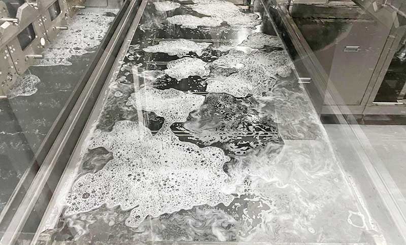
- Strong foam inhibition: low-foam products, ultrasonic cleaning line use, there will be no foam overflow.
3.Technical Parameters
| Product | JH-1015 A | JH-1015 B | Testing Standards |
| Appearance | Colorless to slightly yellow liquid | Colorless to slightly yellow liquid | visual assessment |
| Weight Ratio | 1.150-1.250 | 1.000±0.050 | hydrometer |
| pH Value | ≥14 | 2.0-5.0 | pH Instruments |
| free alkalinity | 300-580mg/L | —— | Company Standards |
If the customer’s demand is within the parameter range of our products, we can specify the corresponding products.


