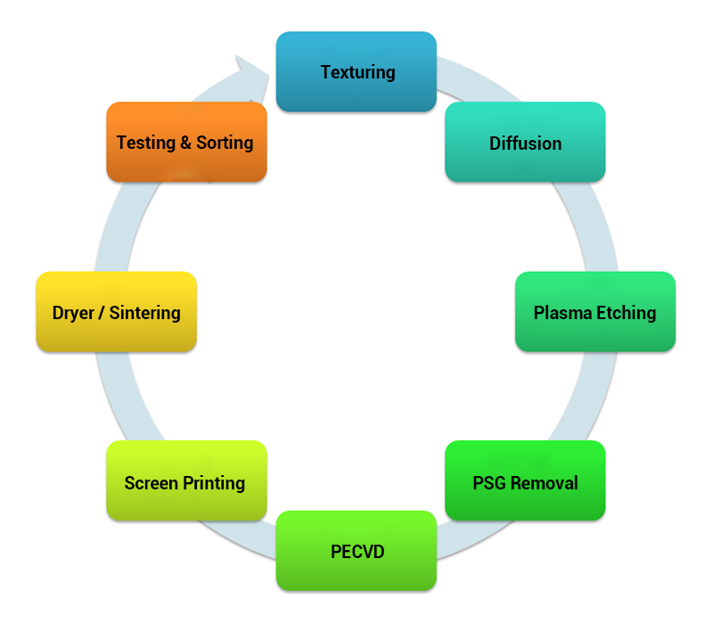
Process 1: silicon wafer cleaning velvet
The preparation of monocrystalline silicon velvet is the use of anisotropic corrosion of silicon, the formation of millions of four-sided square cones per square centimeter of silicon surface that is the pyramid structure. Due to the multiple reflections and refractions of incident light on the surface, the absorption of light is increased, improving the short-circuit current and conversion efficiency of the cell.
Anisotropic corrosion solutions for silicon are usually hot, alkaline solutions; available bases include sodium hydroxide, potassium hydroxide, lithium hydroxide, and ethylenediamine. Mostly, inexpensive, dilute solutions of sodium hydroxide with a concentration of about 1% are used to prepare velvety silicon with an etching temperature of 70-85°C.
In order to obtain uniform velvet, should also be added to the solution of alcohols such as ethanol and isopropanol as a discretionary complexing agent to accelerate the corrosion of silicon. Preparation of velvet before the silicon wafer shall first be preliminary surface corrosion, with alkaline or acidic corrosion solution etched away about 20 ~ 25μm, in the corrosion of velvet, after the general chemical cleaning.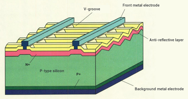
Process 2: Diffusion Junction Making
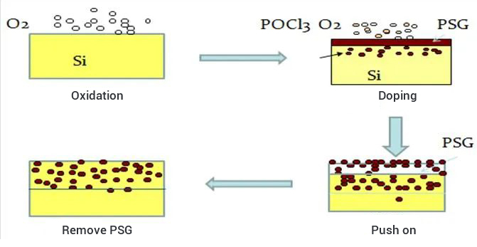
The single/double-sided liquid source phosphorus diffusion of silicon wafers is used to make N-type emitter region to form the basic structure of photoelectric conversion: PN junction. POCl3 liquid molecules are carried into the furnace tube by N2 carrier gas, and after a series of chemical reactions at high temperatures the phosphorus atoms are replaced and diffused into the surface of the silicon wafer, which activates the formation of N-type doping, and forms a PN junction with a P-type substrate. The main chemical reaction formula is as follows:
POCl3+ O2 → P2O5 + Cl2; P2O5+ Si → SiO2 + P
Process 3: Plasma Etching
Since all surfaces of the wafer, including the edges, will inevitably diffuse during diffusion, even if back-to-back diffusion is used, the photogenerated electrons collected on the front side of the PN junction will flow to the back side of the PN junction along the region where the edge diffuses with phosphorus, resulting in a short circuit.
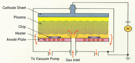
Therefore, the doped silicon surrounding the solar cell must be etched to remove the PN junction from the cell edge. This process is usually accomplished using plasma etching. Plasma etching involves the ionization and formation of a plasma by the parent molecules of the reactive gas CF4 under low pressure and excitation by radio frequency power.
Plasma is composed of charged electrons and ions, the reaction chamber gas in the impact of electrons, in addition to transformed into ions, but also can absorb energy and the formation of a large number of reactive groups. The active reaction groups reach the SiO2 surface due to diffusion or under the action of an electric field, where a chemical reaction occurs with the surface of the material to be etched and a volatile reaction product is formed to detach from the surface of the material to be etched and is pumped out of the chamber by the vacuum system.
Process 4: Removal of Phosphor Silicon Glass
This process is used in the manufacturing process of solar cell wafers, through the chemical corrosion method, i.e., the silicon wafer is placed in hydrofluoric acid solution immersion, so that it produces a chemical reaction to generate soluble complexes and substances of hexafluorosilicic acid, in order to remove a layer of phosphorus silicon glass formed on the surface of the wafer after diffusion of the system junction.
In the diffusion process, POCL3 and O2 reaction to generate P2O5 precipitation on the surface of the wafer, P2O5 and Si reaction to generate SiO2 and phosphorus atoms, so that the formation of a layer of silicon wafer surface containing phosphorus elements of SiO2, called phosphorus silicon glass.
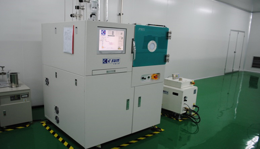
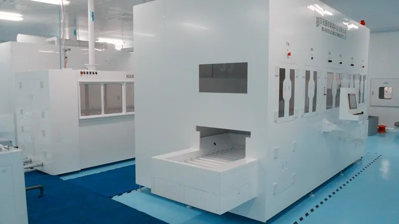
To remove phosphorus silicon glass equipment generally consists of the body, cleaning tank, servo drive system, mechanical arm, electrical control system and automatic acid distribution system and other components, the main power source of hydrofluoric acid, nitrogen, compressed air, pure water, hot exhaust air and wastewater.
Hydrofluoric acid can dissolve silica because hydrofluoric acid reacts with silica to generate volatile silicon tetrafluoride gas. If hydrofluoric acid is in excess, the silicon tetrafluoride generated by the reaction will further react with hydrofluoric acid to generate soluble complexes of hexafluorosilicic acid.
Process 5: Preparation of antireflective film
Suitable materials for anti-reflection layer include titanium oxide (TiO2), silicon nitride (SiNx), silicon monoxide (SiO), aluminum oxide (Al2O3), cesium oxide (CeO2), etc. The chemical vapor deposition (CVD) method is the most commonly used coating technology in the industry. The coating technology of anti-reflective layer, chemical vapor deposition (CVD for short) is most commonly used by the industry, CVD method can be divided into APCVD (Atomspheric Pressure CVD), PECVD (Plasma Enhanced) and RPCVD (Reduced Pressure CVD).
In industry, APCVD and PECVD are commonly used. Physical vapor deposition is also used to make anti-reflective layers, but it is not very popular.
The PECVD method is generally used to produce an anti-reflective layer of silicon nitride (SiNx). In practice, SiH4 and NH3 (or N2) gases are introduced into a reactor to produce an amorphous silicon nitride (SiNx) anti-reflective layer on the surface of silicon crystals. In this antireflective layer, there will be nearly 40% atomic ratio of hydrogen atoms, so although we write the chemical formula of amorphous silicon nitride as SiNx, it should actually be a-SiNx:H.
Process 6: Screen Printing
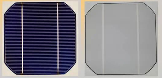
Screen printing is used to complete the production of the back field, back electrode and positive grid line electrode in order to draw out the generated photogenerated current. Process principle: Printing a certain pattern of silver or aluminum paste on the surface of the wafer, forming an ohmic contact through sintering, so that the current can be effectively output;
Positive electrode with Ag metal paste, usually printed into a grid line shape, in order to achieve a good contact at the same time so that the light has a high transmittance; the back side is usually printed with Al metal paste all over the entire back side, one in order to overcome the resistance due to the battery in series, and the second is to reduce the back side of the composite;
Process 7: Sintering
The finished screen printed wafer is placed in a high temperature furnace for the sintering process, the purpose of which is to burn off the organic compounds in the metal paste, and to make the metal particles sintered together to form a good conductor, and at the same time, to take advantage of the high temperature and the surface of the wafer to form a good bonding, the front side of the metal paste is coated on the top of the ARC layer, and the back side of the metal paste is coated on the top of the N-type silicon.
During the sintering process, the active substance in the paste must penetrate the ARC layer and contact the N+ emitter. Therefore, the sintering temperature and time are very important. Excessive sintering will cause silver atoms to penetrate the N+ emitter and enter the P-type substrate at the bottom. On the other hand, insufficient sintering will result in high contact resistance.
Process 8: Inspection and grading
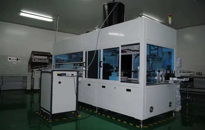
Through the simulation of sunlight pulse irradiation PV cell surface generates photocurrent, photocurrent flows through the simulation load, generating voltage at both ends of the load, the load device will transmit the sampled current, voltage to SCLoad calculation, get IV curve and other indicators. SCLoad according to the test results, according to the given classification rules classification.
Junhe Cell Terminal Fine Chemicals
JUNHE®2550 Monocrystalline cell texturing auxiliary additives
JUNHE®2550 Monocrystalline cell texturing auxiliary additives is a water-soluble, non-toxic and non-hazardous additive that meets the requirements of environmental protection. This product can form micron-level pyramid velvet on the surface of silicon wafers by improving the etching selection ratio of inorganic alkali on silicon, thus achieving good light trapping effect.
1.Features
- Environmental friendly: no need to use IPA and other alcohol products, can achieve selective etching.
- Low production costs: low additive amount, velour production time is only 6-8 minutes, the cost is much lower than IPA velour production process.
- High etching efficiency: Compared with IPA velvet making process, the uniformity of velvet surface and reflectivity is better.
- No initial casting process: greatly reduce the cost of its own additives more environmentally friendly.
2.Technical Parameters
| Compositions | Contents | CAS No. | EC No. |
| Pure water | 95 – 97 % | 7732-18-5 | 231-791-2 |
| Sodium lactate | 2 – 2.5 % | 532-32-1 | 220-772-0 |
| Sodium epoxysuccinate | 1-1 . 5 % | 51274-37-4 | / |
| Surfactant | 0 . 01 – 0 . 05 % | / | / |
| Preservative acid | 0 . 1 % – 0 . 2 % | 137-40-6 | 205-290-4 |
3.Application area
- The product is generally applicable to Perc, Topcon, HJT cell-production process
- It can be applied to all specifications of monocrystalline cells.
JUNHE®2510 Alkali polishing additive for solar cells
JUNHE®2510 monocrystalline cell sheet alkali polishing auxiliary additive for Perc, Topcon solar cell backside alkali polishing and Topcon solar cell de-winding plating, is a water-soluble, non-toxic and harmless additive in line with environmental requirements. This product can greatly improve the corrosion selection ratio of inorganic alkali on silicon dioxide layer and silicon, and greatly reduce the corrosion of inorganic alkali on silicon dioxide layer or PSG layer while realising the polishing and etching of silicon.
1.Features
- Low cost of use:Significantly reduce the amount ofalkali supplement, reduce the cost of materials ; loweramount of additives to meet the needs ofthe factory to reduce consumption.
- Reaction Controllable:More complete pyramid morphology.
- Width ofProduction Window:It can adapt the process temperature of 58-65 °C.
2.Technical Parameters
| Composition | Content | CAS No. |
| Pure water | 85-90% | 7732-18-5 |
| Sodium benzoate | 0.1-0.2% | 532-32-1 |
| Surfactant | 4-5% | ∕ |
| Others | 4-5% | ∕ |
3.Application area
- The product is generally applicable to Perc,Topcon cell-production process.
- Applicable to single crystals of 210, 186, 166, and 158 specifications
JUNHE®2570 Auxiliary additives for removing amorphous silicon of TopCon cells
JUNHE®2570 is a water-soluble, non-toxic and non-hazardous auxiliary additive developed by JUNHE for the removal of amorphous silicon from photovoltaic Topcon cells, which meets the requirements of environmental protection. This product can greatly improve the corrosion selectivity ratio of inorganic alkali to the amorphous silicon winding plating layer of Topcon cell, and greatly reduce the corrosion of inorganic alkali to the positive film silicon dioxide layer or PSG layer while realising the etching of silicon.
1.Features
- Environmental friendly:Selective etching can be achieved without the use of organic bases such as TMAH.
- Low production cost:Compared with the market pre-treatment using hydrofluoric acid / nitric acid, the production cost is greatly reduced.
- High etching efficiency:Compared with Perc cell process, the conversion efficiency is significantly improved.
| Wafer size | Appearance | Photoelectric Conversion | Lifespan |
| 210mm | The etching surface is normal and the positive film has no corrosion. | 24.4%~24.6% | 240+ |
2.Technical Parameters
| First liquid dispensing | Liquid infusion | Intermission-draining | ℃Temperature | Reaction time | |
| 48%KOH | 8~10L | 0.3~0.45L | 5~7L | 63~64 | 100~200 |
| Additive JH2570 | 2.0~4.0L | 0.18~0.21L | |||
| Pure water | 440.0L | / |
These properties may vary depending on the single crystal silicon wafer, process, batch, and size.
3.Application area
- This product is designed for Topcon cell to remove amorphous silicon winding plating process;
- Can be applied to 210, 186, 166, 158mm specifications of the single crystal

